Soldering is a critical step in the production of electronic products, particularly as devices become increasingly complex and surface-mounted components require more precision. The soldering quality has a direct impact on the overall performance of electronic products, and current challenges include lead contamination, cold solder joints, and voids in solder points. These issues jeopardize the reliability of electronic devices and hinder the sustainable growth of the electronics manufacturing industry. Therefore, it is imperative to strengthen research and analysis on soldering reliability for electronic products while implementing effective technical measures to regulate the soldering process scientifically, thus minimizing quality defects and elevating soldering technology standards.
1. Scientific Selection of Solder Materials
The choice of solder materials significantly influences the reliability of soldering in electronic products. Currently, lead-free solder has been widely adopted in the industry due to regulatory requirements and environmental considerations. Such materials must exhibit excellent electrical and mechanical properties, compatibility with existing soldering processes, and good wettability. To prevent lead contamination and electromigration that may undermine soldering reliability, technicians must understand common types of lead-free solder and their characteristics.
In addition to material selection, the use of flux must also be emphasized. Fluxes can be categorized into organic and inorganic types, each serving to dissolve and eliminate oxides from metal surfaces while ensuring that surfaces are effectively covered during the heating process. This isolation from the air reduces oxidation risk and enhances the wettability of solder, ultimately improving soldering reliability. Moreover, attention should be paid to the area and surface condition of the solder joints, with careful control over flux application to ensure high-quality soldering.
2. Optimization of Soldering Processes
Among the most commonly employed soldering techniques in electronic manufacturing are wave soldering and reflow soldering. As component integration density increases and trends towards miniaturization continue, reflow soldering has become the preferred method. However, this process is particularly sensitive to temperature variations, which can compromise soldering reliability.
To address these issues, meticulous temperature control throughout various stages of the reflow process is essential. By analyzing the temperature profile during reflow soldering, adjustments can be made to the preheating, peak temperature, and cooling phases. For instance, during the preheating phase, temperatures should be maintained between 130°C and 180°C with a gradual ramp-up to ensure uniform heating and minimize thermal discrepancies.
In the rapid warming link to warm up the temperature from 180oC to 217oC, it is necessary to effectively use the flux, so that the flux in the full activation of the welding interface after the effective removal of the oxide layer film, the implementation of the implementation of the strengthening of the heating slope control can improve the speed of warming to promote the flux at high temperatures to give full play to the activation of the reaction to avoid the reliability of the weld interface to produce adverse effects; in the reflow Cooling link to the highest peak temperature control within (235 ± 5) oC, and the peak temperature of the reflow zone, peak time and reflow time for a reasonable setup to ensure that the welding operation can form a good solder joints, to be welded after the completion of the cooling rate should be controlled between 3 ~ 5oC / s to prevent the temperature difference is too large to cause damage to the electronic product components.
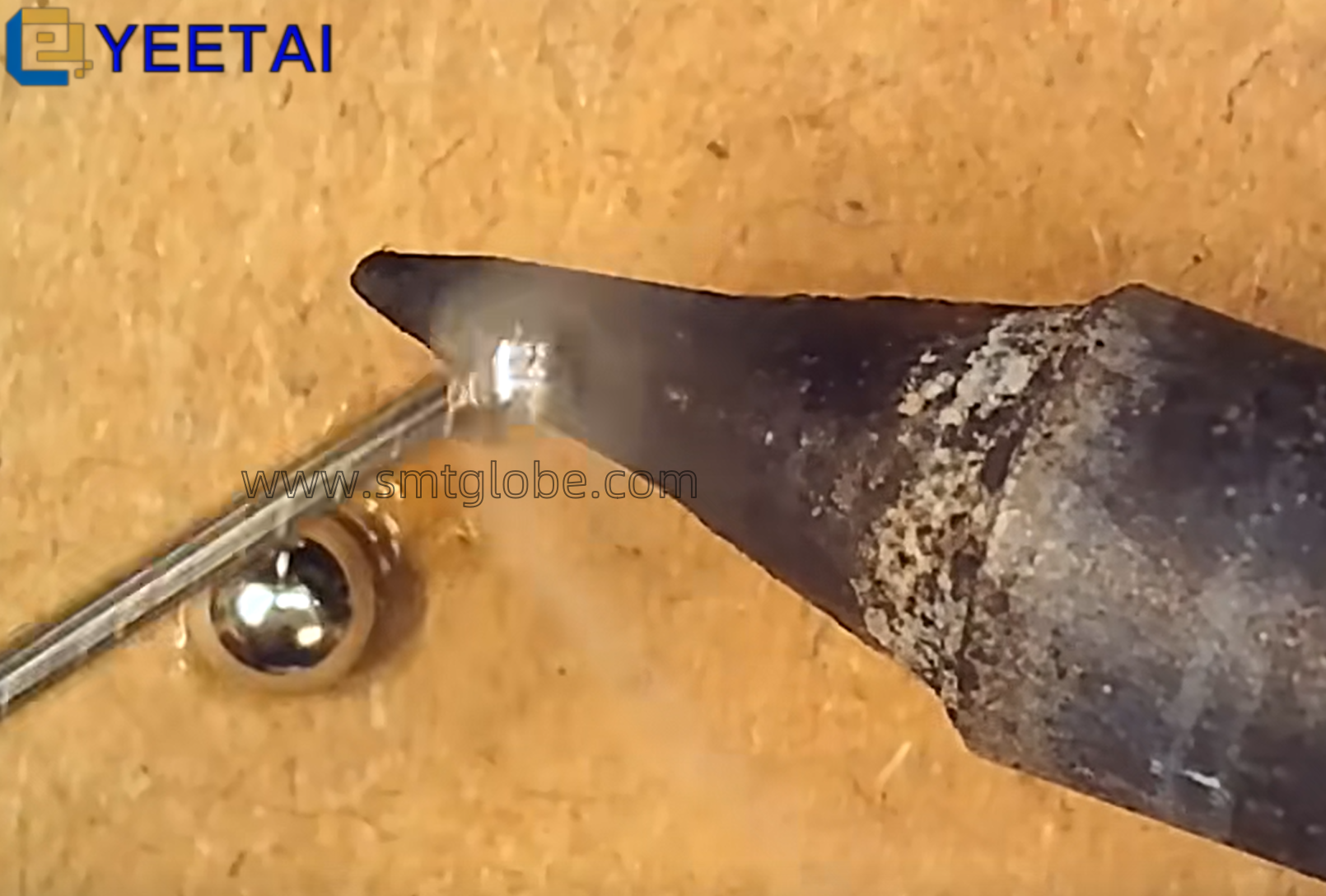
In the welding process optimization and innovation, you can choose more welding processes, such as laser welding, electron beam welding and so on. The former is to heat the surface to be processed by laser radiation, the surface heat spreads to the interior through heat conduction, and by controlling the laser pulse width, energy, peak power and other laser parameters, so that the workpiece melts to form a specific molten pool, with a fast welding speed and a large depth-to-width ratio. The latter is the use of accelerated and focused electron beam bombardment placed in a vacuum or non-vacuum weldments generated by the thermal energy of welding method, because of the advantages of not using welding rods, not easy to oxidize, heat distortion, etc., is widely used in aerospace, electrical and electronic engineering and many other industries. In the selection of these new welding processes to use, but also pay attention to the solder and the fit of these processes to ensure and enhance the quality of welding.
3 Strengthen the quality inspection
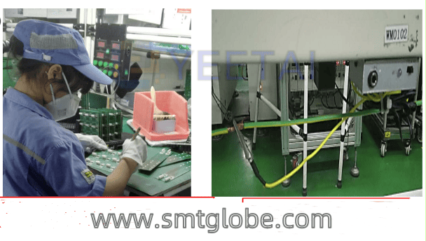
Selection of appropriate testing technology for electronic product welding reliability inspection and analysis, can be found in a timely manner the welding process there are quality defects, and for subsequent amendments to provide strong information support. Practice can be combined with different situations on the artificial visual inspection, automatic optical inspection and other technologies for application, in the application of artificial visual inspection technology, people usually through visual observation, auxiliary microscope and other ways, the size of the larger components of the macroscopic weld inspection, can be observed weld defects bridging, solder paste is not melted, etc., but with the components of electronic products towards the direction of intensive and miniaturized However, as electronic product components toward the direction of intensification and miniaturization, the use of this welded joint quality inspection method will continue to reduce the effect of the need to explore new detection technology to timely find and solve the welding defects. In the application of automatic optical inspection technology, it is well adapted to the component size continues to reduce, PCB board patch density increase and other requirements, the implementation of special inspection instruments can be used through the photoelectricity of the welded joints irradiation, and then use the optical lens on the reflection of the light collection algorithms, after analysis and processing of the computer image processing system, but also to get the results of the scientific judgment of the welding condition of the components for the found For the discovery of solder paste failure, device mounting failure, component welding failure and other problems, can also be intuitive, image to show, in order to provide strong support for the continuous optimization and improvement of subsequent welding operations. In addition, ultrasonic detection method automation, X-ray detection method automation, etc., to realize the effective detection of electronic product welding quality. Among them, through the ultrasonic testing method automation of welding quality inspection, you can through the ultrasonic reflection signal on the components for detailed detection, especially for the IC chip package inside the cavity, delamination and other defects, can be detected through the detection technology in a timely manner, in identifying defects occurring after the real reason, can be in the subsequent welding operations to control and solve. Through the X-ray inspection method automated welding quality inspection, basically can check all the electronic products process defects, the implementation of X-ray can be used to see through the characteristics of the shape of the welded joints to check, and even can be compared with the standard shape of the computer library, in order to scientifically determine the quality of the welded joints.
We can help to simplify and qualify your PTH PCB assembly process. We are also helpful at Through-hole process.
AI Spare parts
SMT AGV Robots
SMT cleaning solutions
solder paste process management